Hardware Development for smart rings, AI smart glasses and AI earbuds by Shenzhen Yt Technology Co.,Ltc.
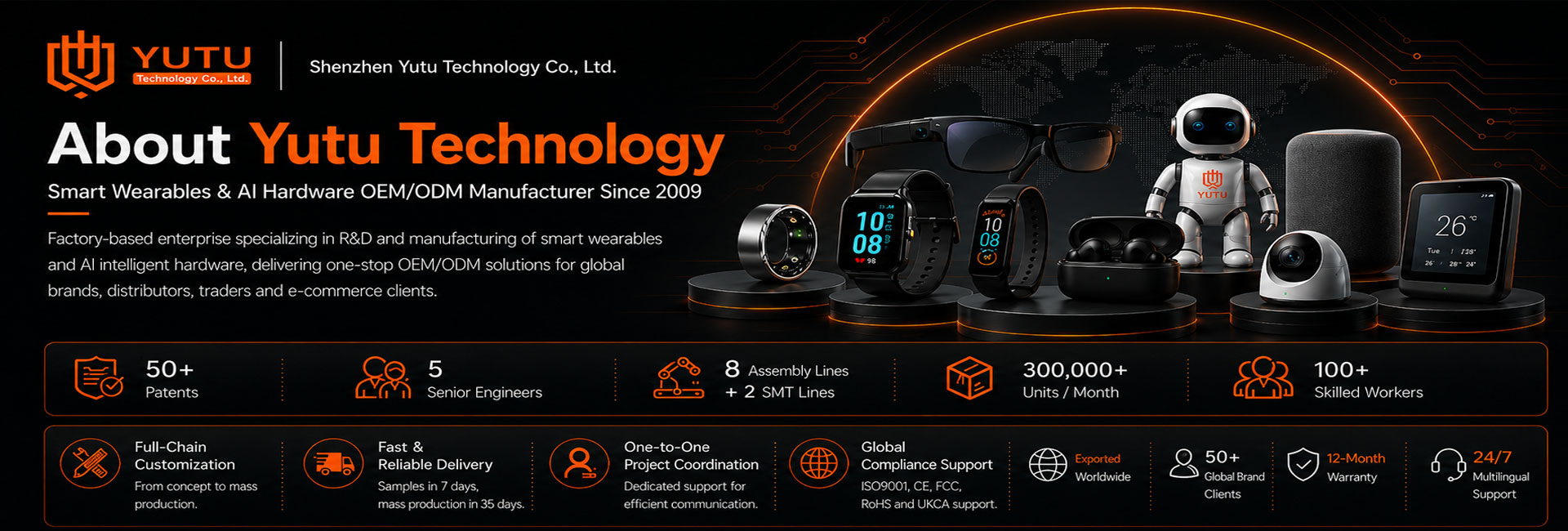
Enterprise Hardware Engineering Since 2009

Precision Hardware Development for AI & Next-Gen Smart Wearables

How Do Global Brands Turn Groundbreaking AI Concepts into Certified, Mass-Produced Wearable Devices? Explore full-lifecycle hardware architecture, ultra-miniature PCB design, low-power sensor integration, and agile manufacturing engineered in Shenzhen.

Precision HDI PCB engineering and micro-battery hardware integration for wearable smart rings
Ultra-Compact Form Factor Engineering

Rigid-Flex & Micro-Sensor Hardware Development

Solving thermal limits, micro-space constraints, and microampere standby currents for biometric health rings and high-density wearable electronics.

Embedded AI hardware development, micro-optical wave-guide engines and acoustic edge computing
Edge Computing & Micro-Optics

Turnkey AI Hardware Development for Vision & Audio

Edge neural processing, beamforming microphone arrays, and optical waveguides engineered directly from schematic design to ISO 9001 SMT lines.

Verified Compliance ISO 9001 CE (RED) FCC ID RoHS UKCA TELEC IP68 Waterproof
Hardware manufacturing since 2009
2009
Hardware Innovation Since
Patents in hardware development
50+
Hardware & Utility Patents
Senior hardware development engineers
5
Senior Chief R&D Directors
SMT and assembly lines for hardware production
8 + 2
Assembly + High-Speed SMT
Monthly hardware production output
300,000+
Monthly Production Capacity
Skilled electronic assembly workforce
100+
Precision Assembly Technicians
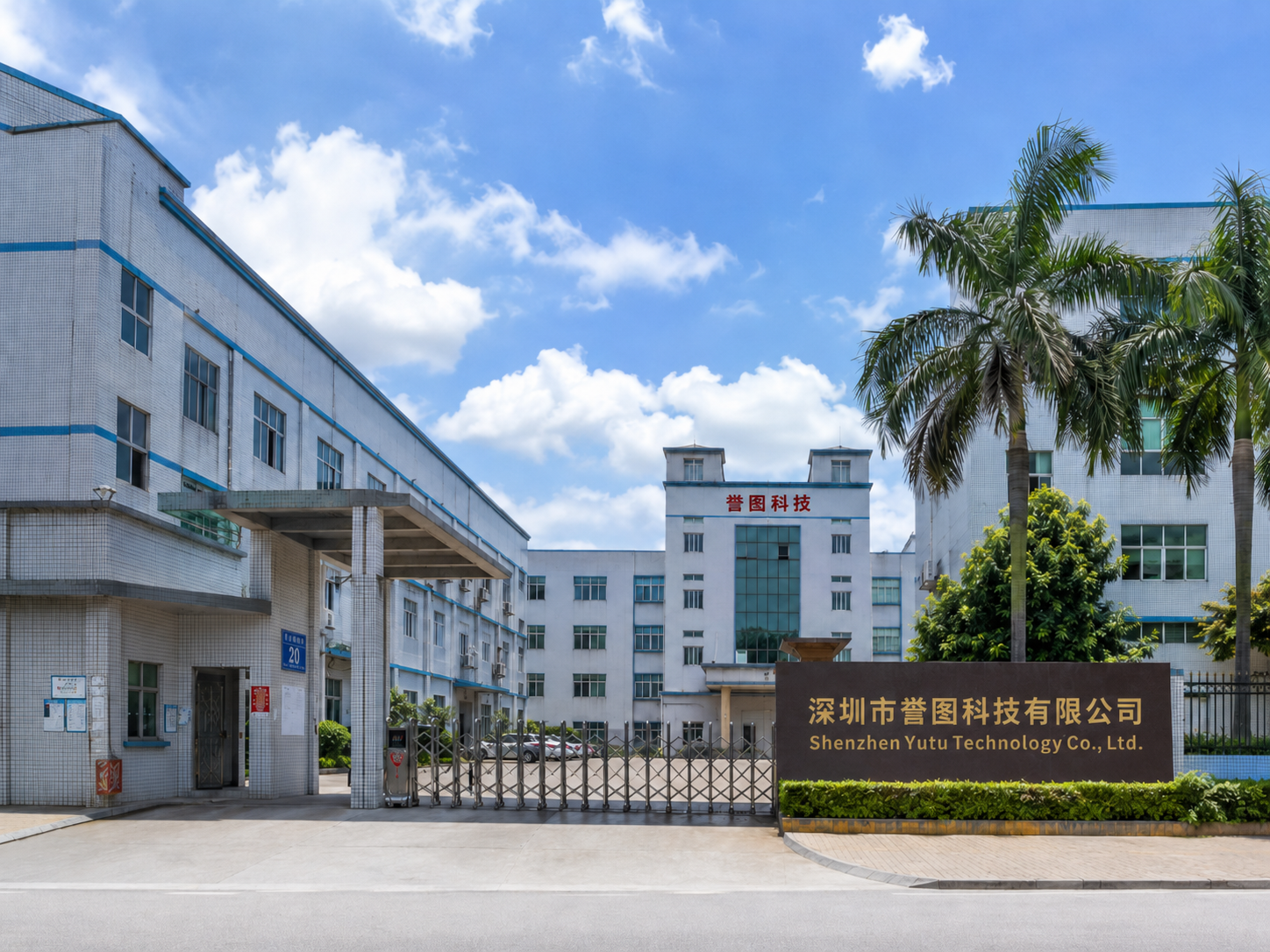
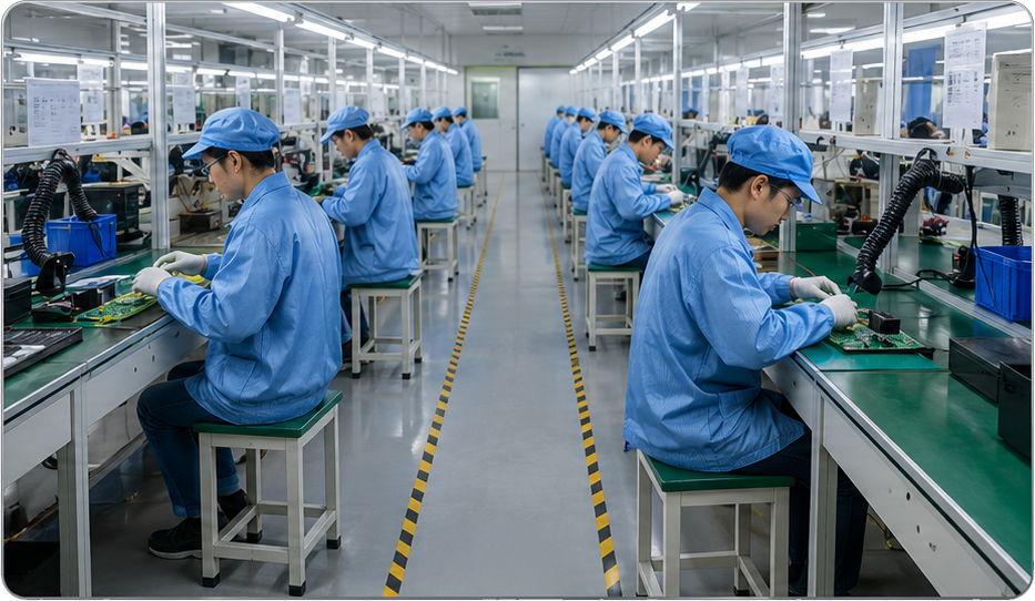
Shenzhen Yt Technology Co.,Ltc. cleanroom SMT production and hardware development facility in Shenzhen
15+Years Continuous
Hardware Innovation
Enterprise Engineering Leadership

Full-Stack Hardware Development: From Schematic Logic to High-Yield Mass Production

In modern consumer electronics and enterprise wearables, robust Hardware Development serves as the fundamental bedrock of user experience, computational throughput, and regulatory approval. Global buyers navigating today's artificial intelligence boom repeatedly face systemic hurdles: thermal dissipation within sub-cubic-centimeter spaces, multi-sensor crosstalk, RF antenna attenuation caused by the human body, and excessive battery drain. Shenzhen Yt Technology Co.,Ltc. solves these multidimensional challenges through a unified engineering methodology established over 15 years in Shenzhen, China.

Unlike broker firms or software studios that subcontract hardware execution, our integrated facility bridges electronic computer-aided engineering (ECAD), mechanical computer-aided engineering (MCAD), firmware development, and automated SMT placement under one ISO 9001 certified roof. By managing schematic design, 8-to-12 layer Any-Layer HDI (High-Density Interconnect) micro-vias, dynamic power-gating architectures, and RF impedance matching in-house, we eliminate the costly iteration cycles that frequently derail new product introductions (NPI).

  • Micro-sensor fusion and low power schematics

    Micro-Sensor Fusion & Power Gating

  • Rigid flex PCB layout and SMT precision

    Rigid-Flex HDI & SMT Assembly

  • Turnkey global compliance testing

    Pre-Compliance RF & DFM Verification

Contact Us
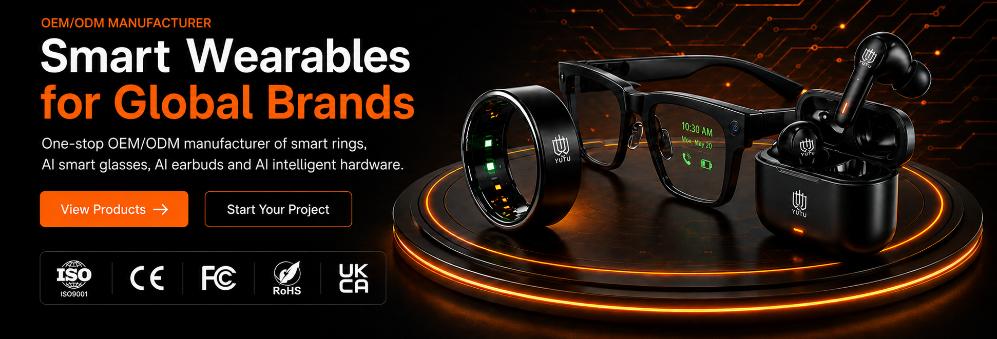
Production-Ready Hardware Platforms

Featured Hardware Development Reference Platforms

Proven, certified baseline architectures ready for immediate private-label branding, customized sensor suites, deep firmware tailoring, and rapid volume manufacturing.

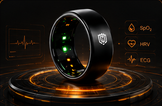
Hardware Development for Health Monitoring Smart Ring

Biometric Smart Ring Hardware Architecture

Engineered for high-density circular form factors. Features ultra-thin multi-layer rigid-flex PCB substrates, green/red/infrared multi-wavelength photoplethysmography (PPG) optical sensor arrays, medical-grade NTC thermistors, and dual-surface dry-contact ECG leads. Controlled via Nordic nRF52840 or low-power Ambiq Apollo microcontrollers with adaptive sampling algorithms delivering 5 to 7 days continuous run-time on a 18mAh solid-electrolyte micro-battery.

  • PPG / SpO2 / HRV
  • Dual-Lead ECG
  • Micro Rigid-Flex HDI
  • 5ATM Waterproofing
  • Inductive Magnetic Charge
Contact Us
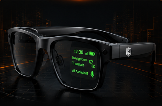
Hardware Development for AI Smart Audio and Display Glasses

AI Smart Glasses Micro-Optical Hardware

Architected with split-temple dual-motherboard topology linked through reinforced micro-coaxial hinge cabling. Integrates high-luminance Micro-LED projection light engines coupled to diffractive optical waveguides (available in monocentric monochrome green or full-color configurations). Includes dual bone-conduction / directional open-ear micro-speakers, quad-beamforming MEMS microphones with neural noise suppression, and integrated BLE 5.3 / Wi-Fi 6 low-power SOCs.

  • Diffractive Waveguide
  • Micro-LED Engine
  • ENC Beamforming Array
  • Touch & IMU Gesture
  • Weight < 42g Chassis
Contact Us
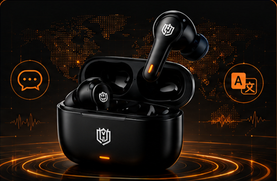
Hardware Development for Real-Time AI Translation and ENC Earbuds

Edge-AI Acoustic & Translation Earbud Platform

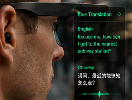
High-precision acoustic hardware featuring bespoke composite diaphragms driven by an ultra-low latency DSP core. Equipped with six feed-forward and feed-back digital MEMS microphones for hybrid 45dB Active Noise Cancellation (ANC) and localized keyword spotting. Optimized for bi-directional live multi-language cloud translation with seamless Bluetooth Dual-Mode audio streaming, automated ear-detection capacitive sensing, and Qi-compatible fast charging cases.

  • Hybrid ANC 45dB
  • Sub-30ms Translation Pipe
  • Spatial Audio DSP
  • LDS Antenna Design
  • Over 30h Combined Play
Contact Us
Engineering Rigor & Stage Gates

The 6-Stage Turnkey Hardware Development Lifecycle

From initial proof-of-concept schematics to high-speed SMT line setups, every project gate incorporates empirical testing, risk mitigation, and Design-for-Manufacturability (DFM) verification.

  1. 01
    Product definition and component selection

    System Architecture & BOM

    Chipset trade-off studies, power budget modeling, key component sourcing, and preliminary BOM target setting.

  2. 02
    Industrial design and ergonomic layout

    ID & Mechanical Integration

    3D packaging ergonomics, CMF specifications, thermal envelope simulation, and structural sealing design.

  3. 03
    Structural engineering and DFM

    Schematic & HDI PCB Layout

    Micro-routing, high-frequency signal integrity, return-path grounding, impedance control, and RF antenna tuning.

  4. 04
    Firmware engineering and protocol integration

    Firmware & Sensor Algorithms

    Bare-metal C/FreeRTOS embedded drivers, low-power sleep modes, secure boot, OTA update chains, and sensor fusion.

  5. 05
    Tooling EVT DVT reliability verification

    EVT, DVT & Pre-Compliance

    Precision tooling, multi-cavity injection molds, drop/vibration stress tests, environmental chambers, and RF pre-scans.

  6. 06
    PVT mass manufacturing and automated quality testing

    PVT & Scaled Mass Production

    Pilot production run, custom functional test fixtures (FCT/ICT), automatic optical inspection (AOI), and global logistics.

Enterprise Manufacturing Advantages

Why Global Tech Brands Trust Shenzhen Yt Technology Co.,Ltc.

Founded in 2009, our organization pairs world-class hardware engineering talent with modern Shenzhen manufacturing infrastructure, giving B2B procurement partners an unfair competitive edge.

Component IQC screening
Component IQC Screening
SMT SPI and AOI inspection
3D-SPI & Dual AOI Checks
Automated functional circuit testing
100% Automated FCT/ICT
Environmental reliability chambers
Reliability & Drop Stress
Outgoing QA audit and packaging
OQA Final Verification
  • ISO 9001 Certified Quality Management System
  • 8 Precision Assembly Lines + 2 High-Speed SMT Lines
  • Overall Production Defect Rate Maintained Below 5‰
  • 50+ Proprietary Hardware & Utility Model Patents
  • Complete Legal IP Protection & Strict Project NDA Protocols
  • Full Turnkey Support: ID, Schematics, Firmware, Mold, APP
SMT automated placement machine and optical quality testing at Shenzhen Yt Technology Co.,Ltc.
Worldwide Footprint & Support

Proven Delivery Across 40+ International Markets

Serving top-tier consumer electronic brands, Kickstarter unicorns, healthcare distributors, and tier-1 retail brands worldwide with reliable manufacturing execution.

Global supply and export network for hardware development projects
40+Countries & Regions Served
60+Active Global Sales Zones
5+Year Sustained Partnerships
24/7Direct Engineering Communication
NDAStrict Intellectual Property Protection
Procurement Engineering FAQ

Frequently Asked Questions on Hardware Development

Comprehensive technical and commercial answers addressing the critical decision criteria encountered by global hardware sourcing directors and engineering executives.

What is the typical timeline and stage-gate process for turnkey hardware development?

A standard custom hardware development lifecycle spans 12 to 20 weeks, systematically structured into discrete stage gates: Phase 1 (Weeks 1–2) encompasses product requirements documentation (PRD), micro-architecture definition, component selection, and initial BOM costing. Phase 2 (Weeks 3–6) covers schematic drafting, HDI PCB layout, and EVT (Engineering Validation Test) functional prototyping with 3D-printed or CNC mechanical enclosures. Phase 3 (Weeks 7–11) executes rapid steel/aluminum injection tooling, DVT (Design Validation Test) builds, automated environmental testing, and preliminary RF/EMC compliance chamber scans. Phase 4 (Weeks 12–16) conducts PVT (Production Validation Test) on the live SMT and assembly line to calibrate test fixtures (ICT/FCT) and verify process capability index (Cpk). Mass production lead time is approximately 35 days post-sample approval.

How do you solve extreme battery life and thermal constraints in miniature wearable hardware?

Thermal and energy mitigation requires tight cross-domain co-design between electronic schematics, PCB layout, and low-level firmware. At the hardware architecture level, Shenzhen Yt Technology Co.,Ltc. utilizes high-efficiency buck-boost DC-DC power management integrated circuits (PMICs) paired with multi-rail power domains. Sensors and non-essential peripherals are isolated via discrete load switches, cutting quiescent leakage current down to sub-3.5 microamperes during standby. In firmware, our embedded engineers design interrupt-driven architectures, sensor FIFO buffering, and adaptive duty cycles so microcontrollers remain in deep sleep modes up to 96% of the operating cycle. Thermally, we utilize multi-ground plane thermal vias, high-emissivity graphite heat spreaders, and conductive epoxy underfills that safely transfer heat toward the outer frame without elevating skin-contact surface temperatures.

How does your factory ensure signal integrity and RF performance on compact wearable devices?

Wearable devices operate in close proximity to lossy biological tissue, which induces severe parasitic loading, detuning, and impedance mismatching on Bluetooth, Wi-Fi, and GNSS antennas. Our engineering team conducts full 3D electromagnetic simulations in CST Studio and Ansys HFSS during layout. We implement Laser Direct Structuring (LDS) or micro-strip ceramic patch antennas integrated directly onto mechanical frame ribs. In addition, our in-house RF lab uses automated network analyzers and anechoic chambers to measure Total Radiated Power (TRP) and Total Isotropic Sensitivity (TIS) using head and hand tissue-equivalent phantoms, guaranteeing robust wireless connectivity within a 15-meter omnidirectional radius.

What international certifications are supported, and who manages the compliance pipeline?

We provide full-turnkey regulatory management for worldwide commercial deployment. Our factory holds an accredited ISO 9001 quality management system certification. We engineer our hardware from the schematic phase to pass CE (RED), FCC ID (Part 15C/15B), RoHS, UKCA, REACH, TELEC (Japan), and battery transportation safety standards (UN38.3, MSDS, IEC 62133). Furthermore, our cleanroom assembly lines support IP68 immersion and 5ATM hydrodynamic pressure sealing protocols. Because we perform pre-compliance emissions and electrostatic discharge (ESD ±8kV contact, ±15kV air) scans in Shenzhen before submitting samples to accredited third-party laboratories (SGS, TUV, BV), our clients achieve first-pass certification rates exceeding 95%.

How do you safeguard client intellectual property, CAD schematics, and firmware source code?

Protecting client IP is our absolute operating policy. Before examining technical documentation, product sketches, or functional specs, Shenzhen Yt Technology Co.,Ltc. executes legally binding bilingual Non-Disclosure Agreements (NDAs). Internally, engineering data is compartmentalized on dedicated, encrypted air-gapped network servers accessible only to project-assigned engineers. Physical prototypes, custom molds, PCB artwork, and Gerber files are uniquely cataloged and never repurposed or exhibited to third parties. Microcontrollers are flashed with locked bootloaders and readout protection (RDP Level 2) during SMT assembly, ensuring firmware cannot be extracted or cloned in downstream channels.

What are the minimum order quantities (MOQs) and scalable production capabilities?

We understand that new hardware innovations require iterative market validation. For customized hardware development and ODM platforms, our standard pilot-run MOQ begins at 1,000 to 2,000 units, allowing brands to launch initial crowdfunding campaigns or pilot distributor trials. Once validated, our factory infrastructure—featuring 8 assembly lines, 2 automated high-speed Panasonic/Yamaha SMT lines, and 100+ skilled operators—seamlessly scales production to 300,000+ units per month to support peak holiday demand and global retail distribution channels.

Start Your Hardware Journey

Accelerate Your Hardware Development with Shenzhen's Premier OEM/ODM Team

Whether you require an architectural consultation for an upcoming biometric smart ring, edge-AI smart glasses, or an industrial IoT wearable, our senior engineering staff is available to evaluate schematic feasibility, optimize your Bill of Materials, and deliver a comprehensive NPI project plan within 24 hours.

Eliminate costly development mistakes, minimize PCB revision spins, and leverage our ISO 9001 certified manufacturing facility to take your product from concept to container shipments.

5 Key Parameters for an Instant Engineering Assessment

Provide these initial technical details to receive an actionable engineering feedback report and preliminary quotation:

  1. 01Form Factor & Mechanical DimensionsWearable ring, optical frames, acoustic enclosure, or custom module
  2. 02Core SOC & Sensor SpecificationsMCU preference (Nordic, Ambiq, Realtek), PPG, ECG, IMU, Micro-display
  3. 03Target Battery Capacity & Endurance ExpectationsOperating runtime, standby current limits, fast-charging requirements
  4. 04Target Compliance & Waterproofing StandardsCE, FCC, RoHS, UKCA, IP68, 5ATM waterproofing depth
  5. 05Project Timeline & Volume ForecastTarget EVT sample date, pilot run quantities, and 12-month volume forecast
Contact Us